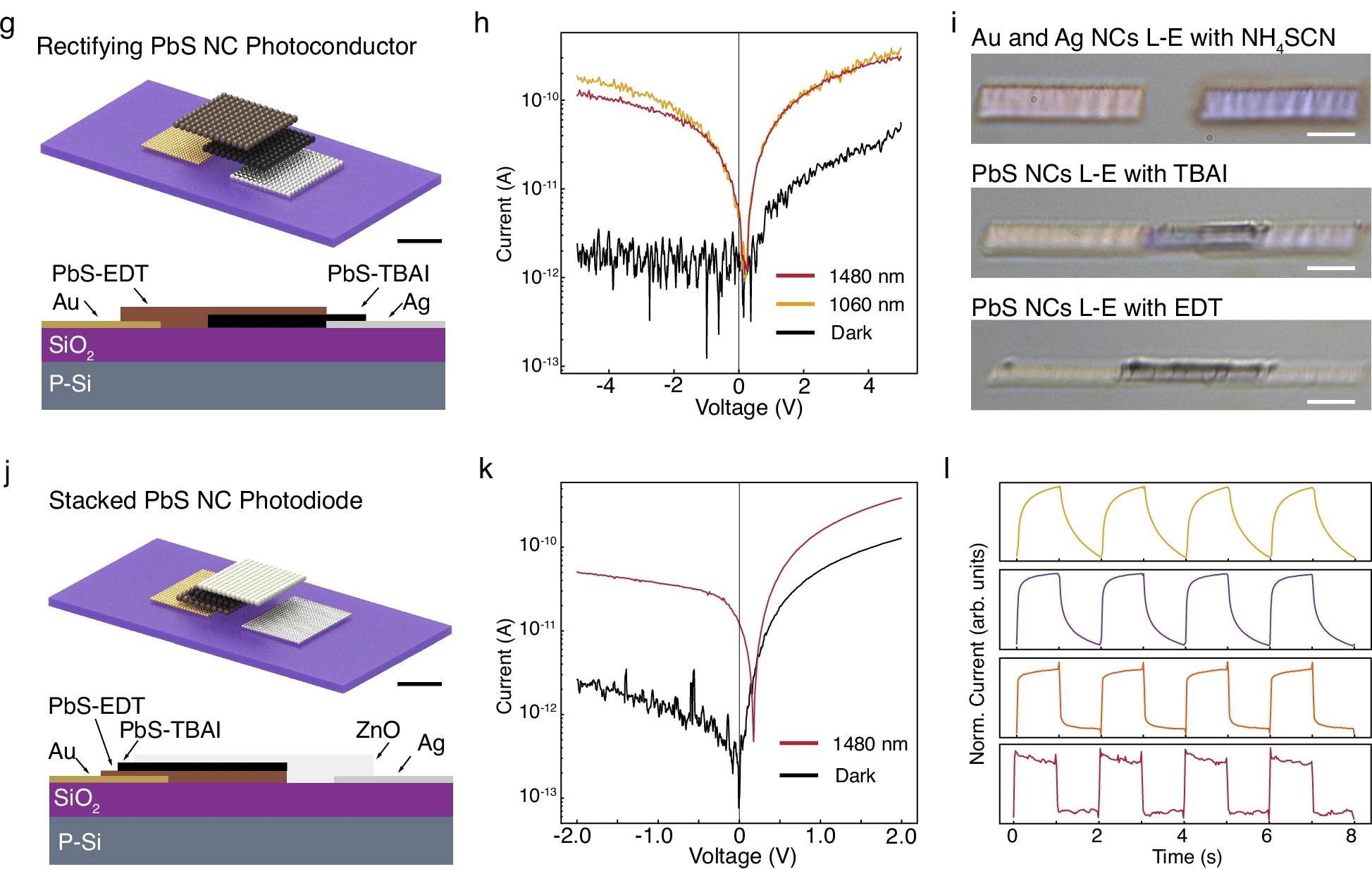
An engineering research team from the Department of Electrical and Electronic Engineering (EEE) at The University of Hong Kong (HKU), led by Professor Leo Tianshuo ZHAO, in collaboration with Professor Ji Tae KIM from the Korea Advanced Institute of Science and Technology (KAIST), has introduced a nano-resolution electrohydrodynamic printing (EHDP) method with room-temperature ligand exchange to fabricate advanced multi-layer (opto)electronic devices. This technique enables precise layer-by-layer printing of nanocrystal (NC) inks, achieving high conductivity and tailored microstructures. By integrating Ag, Au, PbS, and ZnO NCs, they demonstrated fully printed infrared photodiodes with 10-µm pixel sizes and photoresponse to 1500 nm. The method allows versatile material combinations, substrate compatibility, and device architectures, overcoming limitations of inkjet printing and high-temperature sintering. This innovation supports hetero-material and device integration on rigid and flexible substrates, advancing sensing and microelectronics technologies.

^Group photo of HKU engineering research team led by Professor Leo Tianshuo ZHAO.
Article Title:
Ligand-exchange-assisted printing of colloidal nanocrystals to enable all-printed sub-micron optoelectronics
Abstract:
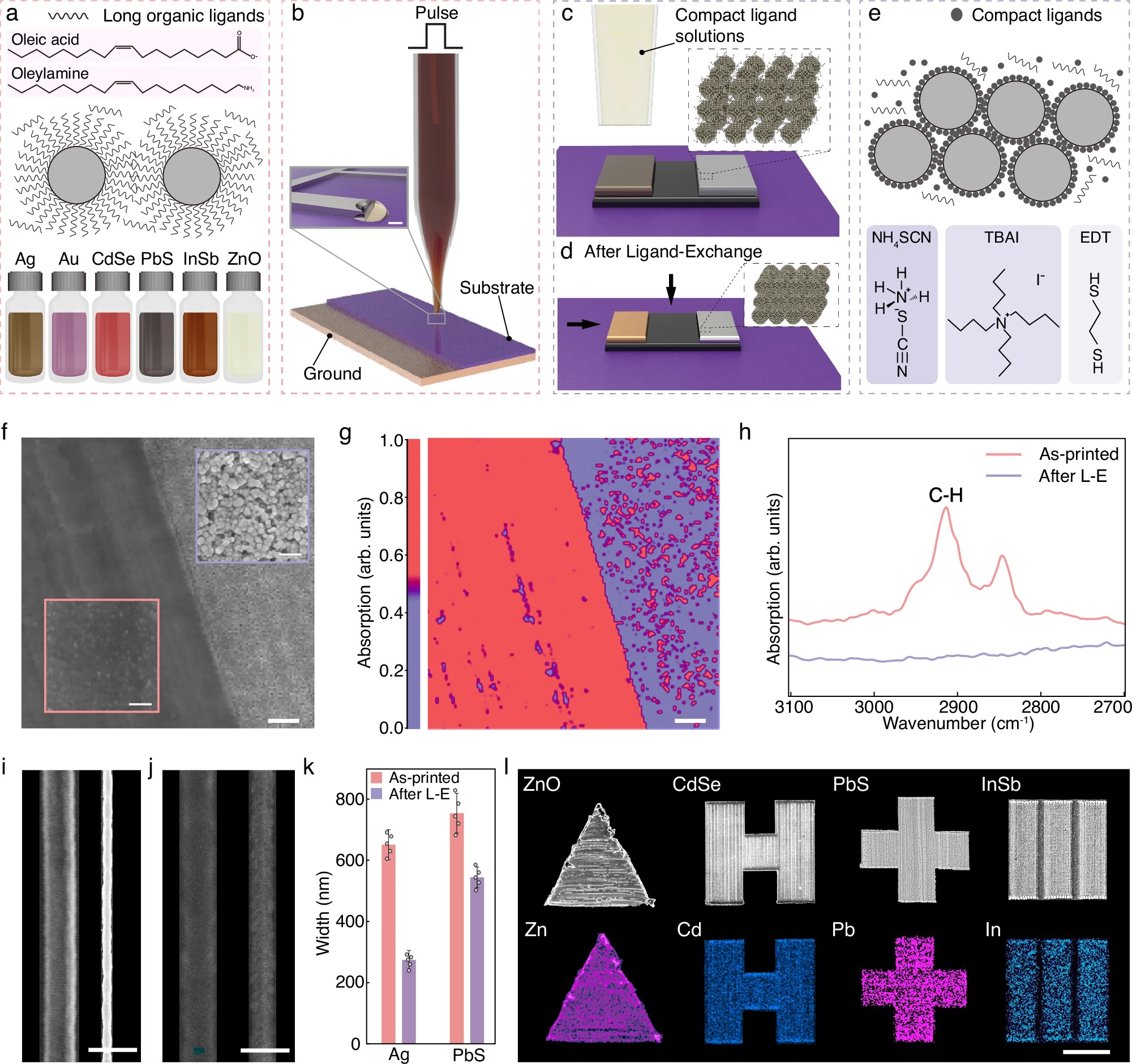
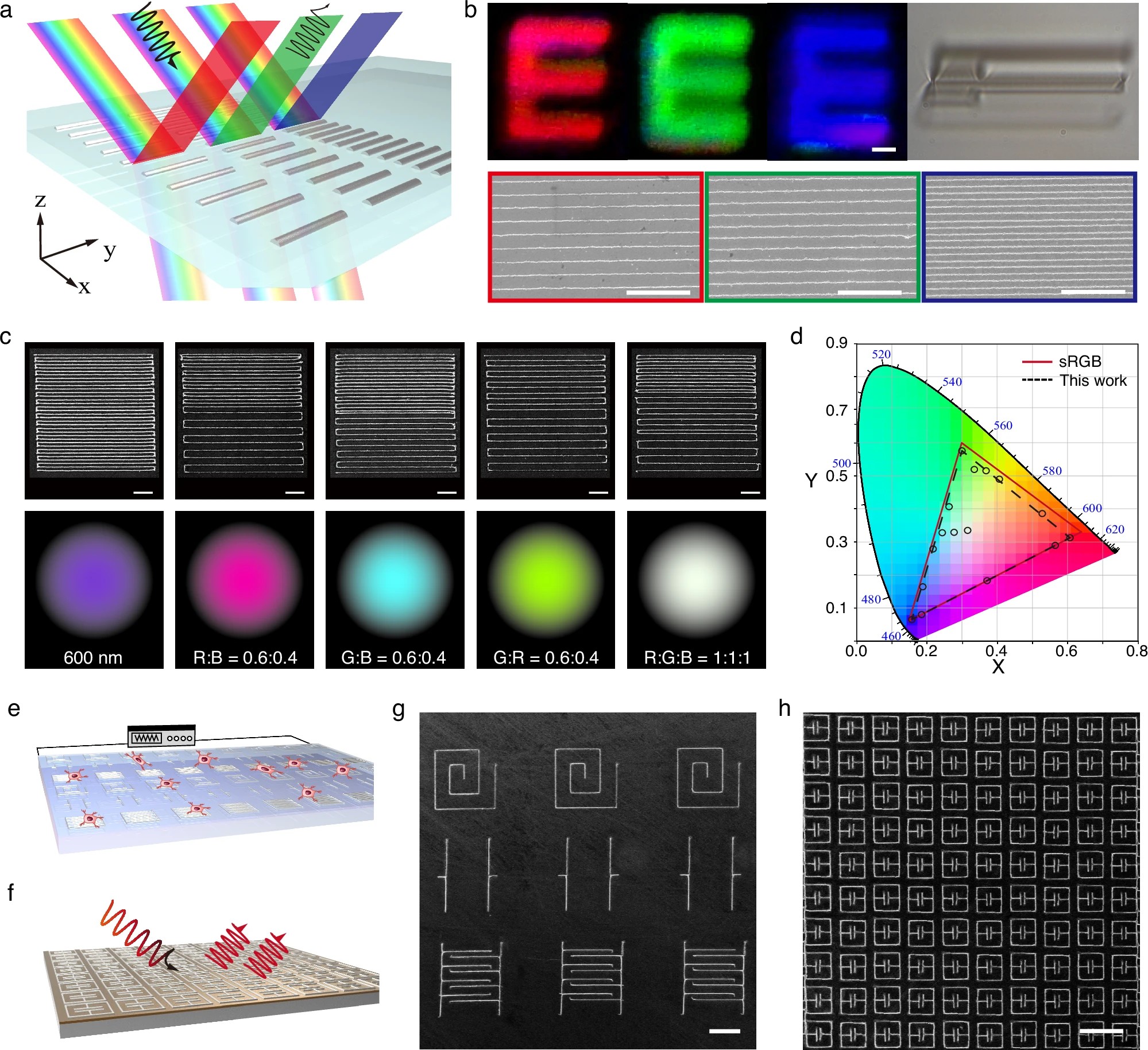
Additive manufacturing enables customised device fabrication for emerging sensing technologies. However, printable (opto)electronic devices with sophisticated architectures, including all-printed photodiodes, face challenges in multi-material and multi-layer printing at micro- and nanoscales with low processing temperatures. Herein, we establish a nano-resolution printing method based on electrohydrodynamic printing (EHDP) to deposit inks from the colloidal nanocrystal (NC) library, followed by in situ room-temperature ligand exchange to functionalise the NC solids. This general approach enables layer-by-layer printing with wide selections of NC inks, ligand reagents, substrates, and device architectures. Chemical-treatment-induced contraction and densification grants printed Ag NC structures electrical conductivity and an achievable feature size and filling ratio of 70 nm and 75%, respectively, constructing wide-gamut structural colour gratings. By exploiting Ag, Au, PbS, and ZnO NCs and compact ligands, we demonstrate all-printed multi-layer infrared photodiodes with sub-10-µm pixel sizes. The nano-printing assembly of hetero-NCs promises the facile integration of multi-functional micro-nano devices.
Article in Nature Communications:
https://www.nature.com/articles/s41467-025-64596-4
NanoMADE Lab @ HKU (Research Group Website):
https://ece.hku.hk/~tszhao